AB07-USB3FMC: The $1.65k eval board they can't be bothered to test
I've written a bit about my look at “commercial off-the-shelf” USB3 PHY boards; and have been taking a look recently at the Design Gateway AB07-USBFMC module. It turns out that my unit has what seems to be a pretty embarrassing defect.
I've been testing my in-progress USB3 gateware with this PHY; and I've been running into an interesting issue: periodically, some of the raw values sent were off by a single bit.
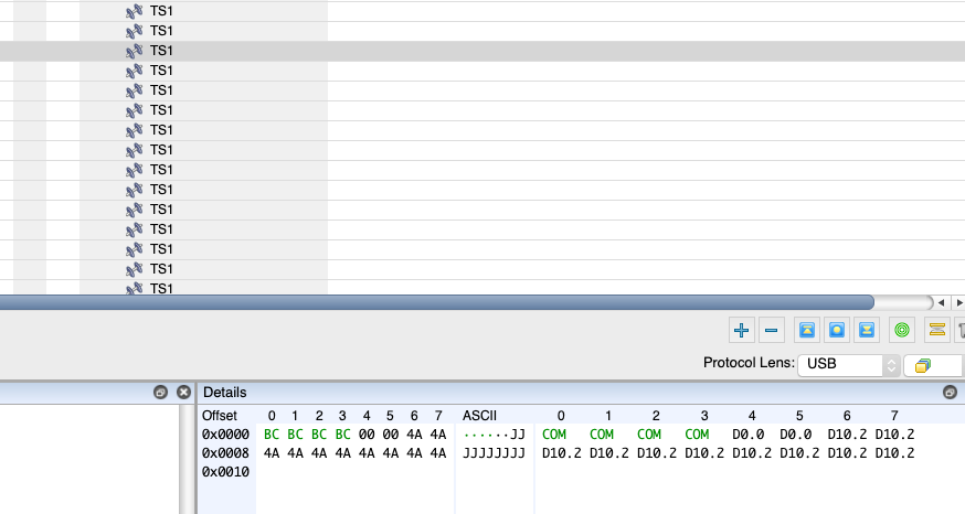
When training a USB3 link, one of the data sequences exchanged looks like this:
BC BC BC BC 00 00 4A 4A
4A 4A 4A 4A 4A 4A 4A 4A
When using the AB07-USBFMC, trying to send this pattern resulted in the following:
BC BC BC BC 00 00 0A 4A
0A 4A 0A 4A 0A 4A 0A 4A
This is interesting for two reasons:
- This PHY has geared inputs, and accepts two bytes of data at a time.
- The incorrect values (
0A) are off from the correct value (4A) by a single bit.
Sure enough, modifying the data packet to send FF instead of 4A pretty clearly shows off that missing bit:
BC BC BC BC 00 00 BF FF
BF FF BF FF BF FF BF FF
At this point, I assumed that I'd gotten the pinout incorrect; and that I'd been writing to the wrong pin – but careful examination of the documentation and my FPGA I/O definitions suggested that I had things right. This suggested it was time to check things on the physical layer.
The board in question looks like this:
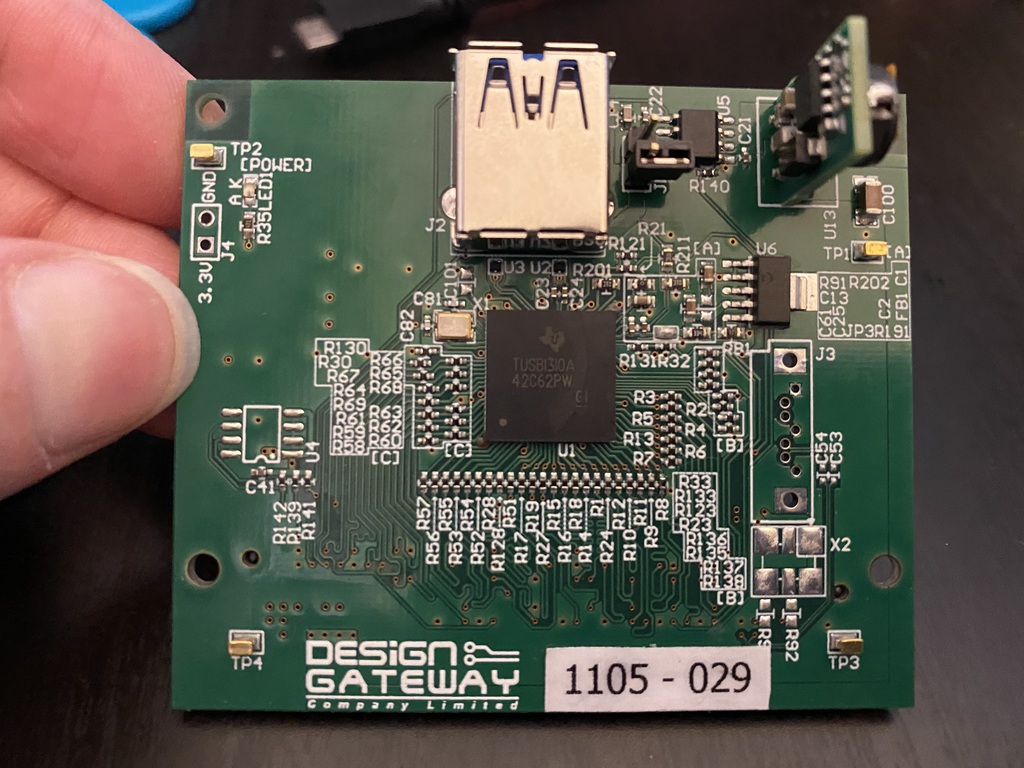
The AB07-USBFMC (slightly modified as detailed later).
Notably, there's a long series of what look like termination / signal conditioning resistors present at the PHY boundary – and it looks like there's about 32 in total; which would make sense: 16 for transmit, and 16 for receive.
A quick probe verifies that these are ~50R resistors, which would make a lot of sense for series termination:
Sure looks like a series termination resistor.
This is excellent news, as it means that the signals are easily accessible without “voiding our warranty”, which is a bit of a comfort when dealing with a rather expensive evaluation board.
So, as a next-step test, I had my FPGA squirt a 100MHz clock signal into every line on the transmit bus, and probed the PHY side of one of those termination resistors:

A nice, healthy wobble. AC coupled.
The frequency and amplitude of this signal are pretty in-line with what you'd expect: the amplitude corresponds
nicely to a decently healthy logic 1. But how does the signal look on the problematic bit?
I adjusted the FPGA design so it only squirted a wave into the problematic bit; and probed in line until I found it:

A *lot* less happy. Still AC couled for display.
Ut-oh. This signal's looking a lot less happy – and a lot more attenuated. At approximately 500mV peak,
you'd be hard pressed to consider this a logic 1, even if you gave it your very best squint. There's no way
this thing would have worked in a test environment – which makes it seem very unlikely that this board was, y'know,
tested.
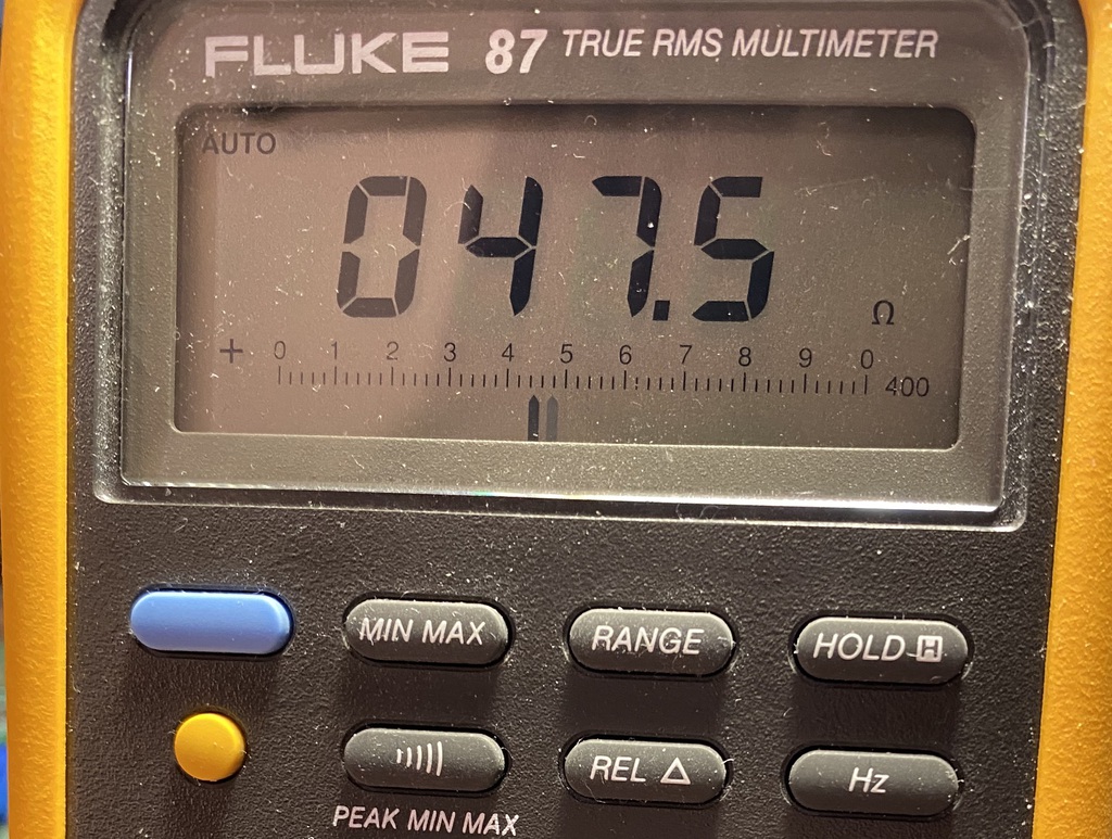
This immediately made me suspicious of the termination resistor sitting next to it; and apparently for good reason:
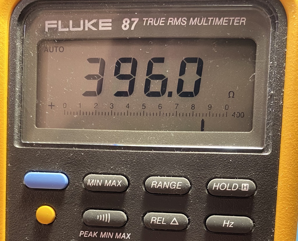
Quite possibly the largest 50 Ω I've ever seen.
This resistor is quite clearly supposed to be 50 Ω. It's also quite clearly not 50 Ω, despite sitting cleanly in the middle of a row of 50 Ω resistors, and pretty much definitely the source of my problems.
So, naturally it's time to perform what I assume must be several hundred dollars worth of rework on this $1.65k board. Luckily, I stock E24 0402s, so I had the resistor replaced with an appropriate value in no time.

Much happier. Note the amplitude.
With an appropriate value replaced, everything looks much happier – and everything works much more nicely. Finally, our USB training sets look just the way they should:
A correct Training Set, at last.
I'm planning on reaching out to Design Gateway – to at least let them know that this is an issue on some boards. I'll update this post if/when I get a reply.