AB07-USB3FMC Notes & Oddities
If you're looking to play with commercial USB3 PHY evaluation hardware – that is, if you're looking to get a board someone else has designed and built, rather than soldering up your own or experimenting with 5G SerDes – there seem to be two options available: the HiTech Global FMC_USB3 ($795 USD), or the Design Gateway AB07-USBFMC ($1,650 USD).

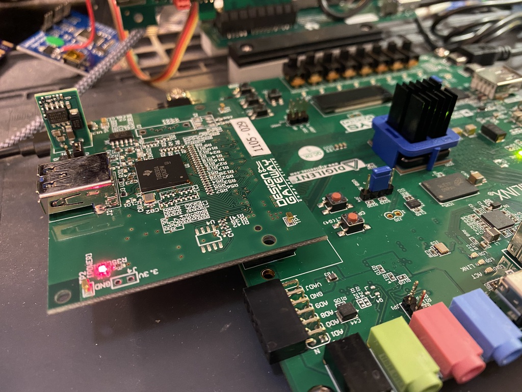
The USB3FMC sitting atop the Digilent Nexys Video FPGA board
Thanks to Tim Ansell, I've been able to get my hands on the AB07-USBFMC; this quick post summarizes my findings so far working with the board.
The Major WTF
It turns out the board I received had a pretty major – but easily correctable – issue: one of its termination resistors was dramatically the wrong size, leaving one out of every sixteen bits sent stuck at zero.
I've documented the whole debacle here for your reading (dis)pleasure.
Other Notes & Findings
- This is essentially a very expensive TUSB1310A breakout board.
- The board is documented only for use with their own USB3 IP core; which means it has some undocumented surprises for anyone who – like me – is running their own USB experiments.
- Despite the TUSB1310A requiring 1V8 signaling; the available board seems to require 2V5 signaling, as it requires a FMC VADJ of 2V5 for its power supply. The excess voltage seems to be dropped down to 1V8 by adding series resistors and letting the ESD protection networks absorb the extra voltage. Probably not great for signal integrity, but eh, it's parallel data at 250MHz.
- The board features a USB-A connector in lieu of a B or C connector. I'd have assumed this is because they're
primarily targeting host gateware, rather than device, but looking at their IP catalog, this doesn't seem to be the
case.
- As a result, in device mode, the TX and RX pairs have their +/- lines swapped. This isn't a problem, per se, as the USB3 specification permits inversion of these pairs, but it can certainly be surprising during debugging.
- There's an unpopulated vertical SATA connector footprint and oscillator footprint on the board. Looking at the
footprints, these seem to go directly to the mezzanine connector; and thus are probably attached to the FPGA's SerDes
lines.
- Amusingly, they go through the effort of “blacking out” these footprints in their reference manual, likely so no one thinks this is also a SATA board.
- Several sets of configuration lines aren't exposed. These don't appear to directly affect functionality, but there
are a few little effects:
- The
TX_ONESZEROESline isn't connected, so one can't use it to generate a quick test/compliance pattern. - The
TX_SWINGlines aren't connected, so one can't artificially limit the transmitter voltage swing. It runs at full swing / “by-the-spec” mode always. - The
ELAS_BUF_MODEline isn't exposed, so the device ostensibly tries to keep its elastic buffer half-full, and doesn't allow use of the TUSB1310A's “nominally empty” mode. - The
RATEline isn't exposed, either, but considering it's supposed to be strapped to1, this seems fine. It is a deviation from the HiTech module, though, and thus worth noting.
- The
I'll add more to this list as I experiment.
In the interim, here's an nMigen connector pinout for the board that I've somewhat tested:
Resource("ab07_usbfmc_pipe", 0,
    # Transmit bus.
    Subsignal("tx_clk",  Pins("FMC_0:LA11_P", dir="o")),
    Subsignal("tx_data", Pins(
        "FMC_0:LA00_CC_P "  # DATA0
        "FMC_0:LA02_P "     # DATA1
        "FMC_0:LA01_CC_P "  # DATA2
        "FMC_0:LA03_P "     # DATA3
        "FMC_0:LA06_P "     # DATA4
        "FMC_0:LA05_P "     # DATA5
        "FMC_0:LA08_P "     # DATA6
        "FMC_0:LA07_P "     # DATA7
        "FMC_0:LA10_P "     # DATA8
        "FMC_0:LA09_P "     # DATA9
        "FMC_0:LA12_P "     # DATA10
        "FMC_0:LA04_P "     # DATA11
        "FMC_0:LA16_P "     # DATA12
        "FMC_0:LA13_P "     # DATA13
        "FMC_0:LA15_P "     # DATA14
        "FMC_0:LA14_P ",    # DATA15
        dir="o"
        )
    ),
    Subsignal("tx_datak", Pins("FMC_0:LA16_N FMC_0:LA15_N", dir="o")),

    # Transmit config.
    Subsignal("tx_elecidle",    Pins("FMC_0:LA09_N",                 dir="o" )),
    Subsignal("tx_detrx_lpbk",  Pins("FMC_0:LA00_CC_N",              dir="o" )),
    Subsignal("tx_deemph",      Pins("FMC_0:LA01_CC_N FMC_0:LA05_N", dir="o" )),
    Subsignal("tx_margin",      Pins("FMC_0:LA03_N ",                dir="o" )),

    # Receive bus.
    Subsignal("pclk",     Pins("FMC_0:LA17_CC_P", dir="i"), Clock(250e6)),
    Subsignal("rx_valid", Pins("FMC_0:LA20_N",    dir="i" )),
    Subsignal("rx_data",  Pins(
        "FMC_0:LA19_P "     # DATA0
        "FMC_0:LA22_P "     # DATA1
        "FMC_0:LA20_P "     # DATA2
        "FMC_0:LA21_P "     # DATA3
        "FMC_0:LA18_CC_P "  # DATA4
        "FMC_0:LA23_P "     # DATA5
        "FMC_0:LA25_P "     # DATA6
        "FMC_0:LA26_P "     # DATA7
        "FMC_0:LA24_P "     # DATA8
        "FMC_0:LA29_P "     # DATA9
        "FMC_0:LA27_P "     # DATA10
        "FMC_0:LA28_P "     # DATA11
        "FMC_0:LA31_P "     # DATA12
        "FMC_0:LA30_P "     # DATA13
        "FMC_0:LA32_P "     # DATA14
        "FMC_0:LA33_P ",    # DATA15
        dir="i"
        )
    ),
    Subsignal("rx_datak",      Pins("FMC_0:LA28_N FMC_0:LA29_N", dir="i")),

    # Receive status/config.
    Subsignal("rx_status",      Pins("FMC_0:LA22_N FMC_0:LA25_N FMC_0:LA23_N", dir="i" )),
    Subsignal("rx_elecidle",    Pins("FMC_0:LA10_N",            dir="io")),
    Subsignal("rx_polarity",    Pins("FMC_0:LA24_N",            dir="o" )),
    Subsignal("rx_termination", Pins("FMC_0:LA18_CC_N",         dir="o" )),

    # Full-PHY Control and status.
    Subsignal("reset",          PinsN("FMC_0:LA02_N",             dir="o" )),
    Subsignal("phy_reset",      PinsN("FMC_0:LA08_N",             dir="o" )),
    Subsignal("power_down",     Pins("FMC_0:LA07_N FMC_0:LA12_N", dir="o" )),
    Subsignal("phy_status",     Pins("FMC_0:LA19_N",              dir="i")),
    Subsignal("pwrpresent",     Pins("FMC_0:LA31_N",              dir="i" )),
    Subsignal("out_enable",     Pins("FMC_0:LA04_N"  ,            dir="o" )),

    # Attributes
    Attrs(IOSTANDARD="LVCMOS25")
),